MOTOSHARE 🚗🏍️
Rent Bikes & Cars Directly from Owners
Motoshare connects vehicle owners with people who need bikes and cars on rent. Owners earn from idle vehicles, and renters get flexible ride options.
Visit Motoshare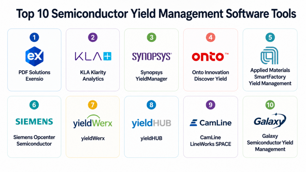
Introduction
Semiconductor Yield Management Software helps chip manufacturers, foundries, OSAT companies, and fabless semiconductor teams understand why wafers, dies, lots, or devices fail during production and testing. In simple terms, it collects manufacturing, inspection, metrology, defect, test, and process data, then turns that data into insights that improve yield, quality, reliability, and production efficiency. As semiconductor designs become more complex and production costs rise, yield improvement is no longer only an engineering task; it is a business-critical priority.
Real World Use Cases
- Wafer yield analysis: Identify patterns across wafers, lots, tools, recipes, and process steps.
- Root cause investigation: Correlate test failures with process, defect, and metrology data.
- Process control: Detect drift, excursions, abnormal behavior, and yield loss early.
- New product ramp: Improve first-pass yield during pilot production and volume ramp.
- Fabless supply-chain visibility: Track quality and yield across foundries, OSATs, and test partners.
Evaluation Criteria for Buyers
- Data coverage: Ability to handle wafer sort, final test, parametric, defect, metrology, MES, and equipment data.
- Analytics depth: Statistical analysis, correlation, root cause analysis, pattern recognition, and AI-assisted insights.
- Integration readiness: Support for MES, EDA, test systems, inspection tools, data lakes, APIs, and enterprise systems.
- Scalability: Ability to process high-volume semiconductor data across fabs, products, and geographies.
- Ease of use: Dashboards, workflow automation, visualization, and usability for engineers.
- Security controls: RBAC, audit logs, access control, encryption, and enterprise authentication.
- Deployment flexibility: Cloud, on-premises, hybrid, or private deployment support.
- Support quality: Semiconductor domain expertise, onboarding, documentation, and professional services.
- Cost and value: Licensing model, implementation cost, customization needs, and long-term ROI.
Best for: Semiconductor fabs, foundries, fabless chip companies, OSAT providers, test engineering teams, process engineers, yield engineers, quality teams, and manufacturing analytics leaders that need deeper visibility into production performance, yield loss, and defect patterns.
Not ideal for: Very small electronics teams, early-stage hardware startups without production data, teams that only need basic spreadsheet reporting, or companies that can solve their needs with simple SPC, MES reporting, or business intelligence dashboards.
Key Trends in Semiconductor Yield Management Software
- AI-assisted yield learning: Modern platforms increasingly use machine learning to detect hidden patterns, classify failures, and suggest likely root causes faster than manual investigation.
- End-to-end data unification: Buyers want one connected view across design, wafer fabrication, assembly, packaging, wafer sort, final test, and field returns.
- Fabless supply-chain analytics: Fabless semiconductor companies need secure visibility across foundries, OSATs, and test partners without owning all production systems directly.
- Advanced packaging complexity: Chiplets, heterogeneous integration, 2.5D packaging, and 3D packaging make yield correlation more difficult and increase demand for multi-step analytics.
- Real-time alerts and excursion detection: Engineering teams want earlier warnings when tool drift, recipe changes, lot anomalies, or test shifts affect yield.
- Hybrid deployment models: Many semiconductor companies prefer private cloud, on-premises, or hybrid deployments because manufacturing data and IP are highly sensitive.
- Integration with data lakes: Yield platforms are increasingly expected to connect with enterprise data platforms, analytics workbenches, and manufacturing data lakes.
- More visual root cause analysis: Engineers need wafer maps, pareto charts, trend charts, correlation plots, defect maps, and automated drill-downs in one workflow.
- Automation of engineering workflows: Repeatable analysis templates, automated reports, and rule-based workflows reduce manual work for yield and product engineers.
- Security and IP protection: Semiconductor manufacturing data contains process recipes, product performance, and proprietary design information, so access control and auditability are now critical buying factors.
How We Selected These Tools
- We prioritized platforms that are recognized in semiconductor manufacturing, yield analytics, test analytics, process control, or manufacturing intelligence.
- We looked for tools that support semiconductor-specific data such as wafer maps, probe data, final test data, defect data, metrology data, lot genealogy, and process history.
- We considered feature completeness across analytics, visualization, correlation, root cause analysis, reporting, and workflow automation.
- We included a mix of enterprise-grade platforms, fabless-focused analytics tools, manufacturing execution ecosystems, and specialized yield management products.
- We evaluated practical buyer fit across IDMs, foundries, OSATs, fabless companies, and advanced packaging environments.
- We gave higher consideration to platforms with strong integration potential across MES, equipment, test, inspection, and enterprise data systems.
- We avoided guessing public ratings, certifications, or pricing details where they are not clearly available.
- We considered scalability, support ecosystem, implementation complexity, and semiconductor domain relevance.
- We included tools that can support modern yield learning, production monitoring, and continuous improvement workflows.
- The scoring is comparative and practical, not a claim of absolute product superiority.
Top 10 Semiconductor Yield Management Software Tools
1- PDF Solutions Exensio
Short description:
PDF Solutions Exensio is a semiconductor analytics platform built for yield improvement, manufacturing analytics, test analytics, and product engineering workflows. It is widely used by semiconductor companies that need to connect large volumes of manufacturing and test data into one analytics environment. The platform is especially strong for IDMs, foundries, fabless semiconductor companies, and OSAT-driven workflows where yield learning depends on cross-functional data correlation. It helps teams analyze product performance, identify yield loss patterns, and accelerate production ramp. Exensio is best suited for companies with complex manufacturing data and strong engineering analytics requirements.
Key Features
- Semiconductor manufacturing analytics and yield ramp support
- Test, product, and process data correlation
- Wafer map analysis and engineering dashboards
- Root cause analysis for yield loss and product issues
- Support for large-scale semiconductor data environments
- Workflow support for product, yield, and test engineering
- Enterprise analytics for fabless, IDM, and foundry use cases
Pros
- Strong semiconductor-specific analytics depth for yield and manufacturing teams.
- Suitable for complex, high-volume production and product ramp environments.
- Useful for cross-functional teams working across test, yield, product, and process engineering.
Cons
- May require significant implementation planning and data integration work.
- Best value is usually achieved by mature semiconductor organizations with enough production data.
- Pricing and deployment details may vary based on enterprise requirements.
Platforms / Deployment
Web / Windows / Linux
Cloud / Self-hosted / Hybrid may vary by customer environment
Security & Compliance
Enterprise security features may vary by deployment.
RBAC, authentication controls, and data access governance are commonly expected in enterprise semiconductor environments.
Specific certifications are Not publicly stated.
Integrations & Ecosystem
Exensio is designed to work within semiconductor manufacturing and product engineering ecosystems where data comes from multiple internal and external sources. It can support analytics across test, manufacturing, product, and engineering data flows.
- MES and manufacturing databases
- Wafer sort and final test data
- Product engineering data sources
- Foundry and OSAT data feeds
- Defect, metrology, and process data
- Enterprise analytics and reporting environments
Support & Community
PDF Solutions provides enterprise-focused support, onboarding, implementation guidance, and semiconductor domain expertise. Community visibility is more enterprise and customer-driven than open community-based. Support depth usually depends on licensing, project scope, and customer engagement model.
2- KLA Klarity Analytics
Short description:
KLA Klarity Analytics is designed for semiconductor process control, defect analytics, inspection data analysis, and yield improvement workflows. It is especially relevant for fabs and manufacturing teams that already rely heavily on inspection, metrology, and process control data. The platform helps engineers connect defect signals with yield outcomes and process behavior. It is suitable for advanced manufacturing environments where defect density, process excursions, and wafer-level variation need close monitoring. Klarity Analytics is often considered a strong fit for enterprise fabs and process engineering teams.
Key Features
- Defect and inspection data analytics
- Process control and yield improvement workflows
- Wafer-level visualization and trend analysis
- Root cause analysis for process excursions
- Integration with inspection and metrology ecosystems
- Manufacturing intelligence for fabs and process teams
- Support for advanced semiconductor process monitoring
Pros
- Strong alignment with defect inspection and process control workflows.
- Valuable for fabs that need tight connection between metrology, inspection, and yield.
- Suitable for high-volume semiconductor manufacturing environments.
Cons
- May be more complex than needed for smaller or fabless-only teams.
- Best fit is often within KLA-heavy or advanced fab environments.
- Implementation may require specialized process and data engineering support.
Platforms / Deployment
Web / Windows / Linux
Cloud / Self-hosted / Hybrid varies by enterprise deployment
Security & Compliance
Enterprise access control, secure data handling, and role-based workflows are expected in large fab environments.
Specific public compliance certifications for this product are Not publicly stated.
Integrations & Ecosystem
Klarity Analytics fits naturally into semiconductor process control and inspection environments, especially where defect, metrology, and equipment data are central to yield learning.
- Inspection systems
- Metrology systems
- Process control platforms
- MES and fab data systems
- Wafer defect review workflows
- Engineering analytics repositories
Support & Community
KLA has a strong semiconductor equipment and process control ecosystem, which supports enterprise customers through technical services, application engineering, and domain-specific expertise. Public community resources are limited compared with open-source tools, but enterprise support is typically strong.
3- Synopsys YieldManager
Short description:
Synopsys YieldManager is a yield management and manufacturing analytics solution focused on helping semiconductor teams manage large volumes of production data and identify causes of yield loss. It is designed to support consistent analysis across fabs and engineering teams. The platform helps engineers correlate data from multiple sources, visualize yield behavior, and reduce time spent searching manually for root causes. It is useful for organizations that need structured yield workflows and repeatable analysis methods. YieldManager is a strong option for teams that want semiconductor-specific analytics connected to broader design-to-manufacturing workflows.
Key Features
- Yield data management and analysis
- Common data framework for manufacturing analytics
- Cross-source correlation and statistical analysis
- Visualization for yield trends and failure patterns
- Support for multi-team engineering collaboration
- Root cause analysis for yield issues
- Semiconductor-focused data analysis workflows
Pros
- Strong semiconductor engineering orientation.
- Useful for organizations that need consistent analysis methods across teams.
- Can help reduce manual effort in yield problem investigation.
Cons
- May require mature data pipelines and clean manufacturing data.
- Advanced value depends on integration quality across production systems.
- Pricing and deployment details are usually enterprise-specific.
Platforms / Deployment
Web / Windows / Linux
Cloud / Self-hosted / Hybrid varies by implementation
Security & Compliance
Not publicly stated.
Enterprise customers should validate SSO, RBAC, encryption, audit logs, and data residency requirements during evaluation.
Integrations & Ecosystem
YieldManager is positioned around semiconductor manufacturing analytics and yield data correlation. It can fit into engineering environments where multiple data sources must be analyzed consistently.
- Fab manufacturing data
- Test and wafer sort data
- Defect and metrology datasets
- MES and process systems
- Engineering dashboards
- Data repositories and analytics platforms
Support & Community
Synopsys has a strong semiconductor software ecosystem and enterprise customer support model. Support may include documentation, technical support, professional services, and account-based assistance. Community discussion is more specialized and enterprise-oriented.
4- Onto Innovation Discover Yield
Short description:
Onto Innovation Discover Yield is a yield management platform focused on parametric, defect, and yield optimization. It is designed for semiconductor manufacturing teams that need to connect data mining, workflow development, and yield analysis across manufacturing data sources. The platform is particularly useful for engineering teams analyzing defect patterns, parametric shifts, and process-related yield loss. It supports data-driven improvement across memory, logic, assembly, and packaging workflows. Discover Yield is a strong fit for organizations that need fab-wide yield visibility and practical engineering analytics.
Key Features
- Parametric yield analysis
- Defect and yield optimization
- Data mining and workflow development
- Cross-source semiconductor data analysis
- Support for fab, assembly, and packaging data
- Engineering visualization and reporting
- Yield improvement workflows for process teams
Pros
- Strong fit for defect, parametric, and yield correlation use cases.
- Useful across manufacturing, assembly, and packaging environments.
- Practical for engineering teams focused on process improvement.
Cons
- May require integration effort with existing data sources and fab systems.
- Best suited for organizations with dedicated yield engineering workflows.
- Public pricing and detailed compliance information are limited.
Platforms / Deployment
Web / Windows / Linux
Cloud / Self-hosted / Hybrid varies by enterprise environment
Security & Compliance
Not publicly stated.
Buyers should confirm identity management, access control, audit logs, encryption, and deployment security during procurement.
Integrations & Ecosystem
Discover Yield is designed to work across semiconductor data sources, including process, defect, parametric, and packaging information. It fits well where yield teams need structured workflows and data mining capabilities.
- Defect inspection data
- Parametric test data
- Wafer-level manufacturing data
- Assembly and packaging data
- Engineering workflow systems
- Fab data repositories
Support & Community
Onto Innovation provides enterprise and technical support aligned with semiconductor process and yield workflows. Documentation, onboarding, and support depth may vary by contract and deployment model.
5- Applied Materials SmartFactory Yield Management
Short description:
Applied Materials SmartFactory Yield Management is part of a broader smart manufacturing ecosystem for semiconductor fabs. It helps engineers improve yield learning, manage fab-wide yield data, and accelerate production ramp. The platform is relevant for manufacturers that need connected factory intelligence across equipment, process, defect, and production data. It supports data-driven decision-making for process engineers, yield engineers, and manufacturing teams. SmartFactory Yield Management is best suited for fabs looking for an integrated manufacturing and yield improvement environment.
Key Features
- Fab-wide yield data management
- Yield learning and production ramp support
- Defect and process data analytics
- Manufacturing workflow integration
- Engineering dashboards and reporting
- Support for smart factory initiatives
- Integration with semiconductor production environments
Pros
- Strong fit for large fabs and manufacturing operations.
- Useful when yield management is part of broader smart factory transformation.
- Can support connected workflows between engineering and manufacturing teams.
Cons
- May be too enterprise-heavy for small fabless organizations.
- Implementation can require coordination across manufacturing systems.
- Product details may vary by customer deployment and solution package.
Platforms / Deployment
Web / Windows / Linux
Cloud / Self-hosted / Hybrid varies by implementation
Security & Compliance
Not publicly stated.
Enterprise semiconductor buyers should validate RBAC, audit logs, encryption, SSO, and data governance requirements directly.
Integrations & Ecosystem
SmartFactory Yield Management is designed for integrated semiconductor manufacturing operations where yield data connects with factory systems and process workflows.
- MES and factory systems
- Defect management systems
- Process and equipment data sources
- Manufacturing dashboards
- Engineering analytics tools
- Smart factory applications
Support & Community
Applied Materials has a large semiconductor manufacturing ecosystem and enterprise support structure. Support is typically project-based and may involve implementation specialists, application engineers, and long-term technical account support.
6- Siemens Opcenter Semiconductor
Short description:
Siemens Opcenter Semiconductor is an enterprise manufacturing operations platform that supports semiconductor production, process visibility, quality, and manufacturing analytics. While it is broader than standalone yield management software, it can play an important role in yield improvement by connecting manufacturing execution, process data, production tracking, and analytics workflows. It is especially useful for semiconductor manufacturers that want MES, production intelligence, and yield-related insights in one operational ecosystem. Siemens Opcenter is best suited for large manufacturers that need scalable factory operations and enterprise integration.
Key Features
- Semiconductor manufacturing execution support
- Production tracking and operational visibility
- Quality and process management workflows
- Manufacturing analytics and reporting
- Integration with enterprise and shop-floor systems
- Support for complex production environments
- Scalable architecture for multi-site operations
Pros
- Strong fit for enterprises that need manufacturing operations and yield visibility together.
- Good ecosystem for companies already using Siemens industrial software.
- Useful for standardizing production and quality workflows across sites.
Cons
- Not purely a specialized yield analytics tool.
- Implementation can be complex for organizations without mature operations architecture.
- May require additional analytics layers for advanced yield engineering needs.
Platforms / Deployment
Web / Windows / Linux
Cloud / Self-hosted / Hybrid varies by Siemens solution and customer environment
Security & Compliance
Enterprise-grade security capabilities may vary by deployment.
Specific certifications for this exact use case are Not publicly stated. Buyers should validate SSO, RBAC, encryption, auditability, and compliance needs.
Integrations & Ecosystem
Siemens Opcenter integrates into broader manufacturing and enterprise technology stacks, making it useful where yield management must connect with MES, PLM, ERP, and automation systems.
- MES and production systems
- PLM and engineering systems
- ERP and planning tools
- Industrial automation systems
- Quality management workflows
- Analytics and reporting platforms
Support & Community
Siemens offers enterprise support, implementation partners, documentation, and professional services. The ecosystem is strong for large industrial and manufacturing customers, but configuration and rollout may require experienced partners.
7- yieldWerx
Short description:
yieldWerx is a semiconductor yield analytics and quality management platform focused on predictive analytics, traceability, automation, and end-to-end visibility. It is useful for fabless companies, IDMs, and semiconductor teams that need to unify test, process, defect, reliability, and manufacturing data. The platform emphasizes AI-assisted analytics, real-time alerts, root cause analysis, and data quality monitoring. It can help teams detect process variation, compare lots, and manage yield across supply-chain partners. yieldWerx is a practical option for teams looking for modern analytics with a strong semiconductor yield focus.
Key Features
- AI-assisted predictive yield analytics
- End-to-end semiconductor data repository
- Root cause analysis and failure correlation
- Real-time alerts and health monitoring
- Fab-to-assembly and test correlation
- Lot genealogy and traceability
- Support for fabless, IDM, and manufacturing workflows
Pros
- Strong focus on semiconductor yield, quality, and traceability.
- Useful for fabless companies needing visibility across supply-chain partners.
- Modern analytics approach with automation and predictive capabilities.
Cons
- Enterprise implementation may still require careful data mapping.
- Public pricing and detailed security certifications are not broadly available.
- May need customization for highly complex legacy environments.
Platforms / Deployment
Web
Cloud / Hybrid / Self-hosted may vary by customer requirements
Security & Compliance
Security-focused messaging is publicly emphasized, but specific certifications are Not publicly stated.
Buyers should confirm SSO, MFA, encryption, RBAC, audit logs, and data residency needs during evaluation.
Integrations & Ecosystem
yieldWerx is designed to unify heterogeneous semiconductor data across manufacturing, test, quality, and supply-chain workflows. It is especially relevant where data comes from multiple internal and external partners.
- Wafer sort and final test data
- Process and defect data
- Metrology and critical dimension data
- Assembly and packaging data
- System-level test data
- Quality and RMA data sources
Support & Community
Support is vendor-led and semiconductor domain-focused. Documentation, onboarding, customer success, and implementation guidance are expected to vary by customer scope. Public community visibility is limited, but product focus is highly specialized.
8- yieldHUB
Short description:
yieldHUB is a semiconductor yield management and test analytics platform used by product engineers, test engineers, and quality teams. It focuses on making semiconductor test data easier to analyze, visualize, and share. The platform is practical for fabless companies and test-driven teams that need dashboards, wafer maps, yield reports, and engineering analytics without building everything internally. It can support faster debugging, customer reporting, and production monitoring. yieldHUB is a strong fit for teams that want accessible yield analytics with a focus on semiconductor test data.
Key Features
- Semiconductor test data analytics
- Yield dashboards and reporting
- Wafer map visualization
- Product and lot-level analysis
- Engineering collaboration workflows
- Support for fabless and test engineering teams
- Production monitoring and quality insights
Pros
- Practical and focused for test and product engineering teams.
- Easier to adopt than some large enterprise fab platforms.
- Useful for fabless semiconductor organizations and distributed engineering teams.
Cons
- May not provide the same fab-wide process control depth as large enterprise platforms.
- Advanced integrations depend on data availability and customer setup.
- Some enterprise security and compliance details are Not publicly stated.
Platforms / Deployment
Web
Cloud / Hybrid / Self-hosted varies by customer environment
Security & Compliance
Not publicly stated.
Buyers should validate access control, encryption, audit logs, SSO, and data handling policies during procurement.
Integrations & Ecosystem
yieldHUB is commonly relevant where semiconductor test data, wafer maps, product data, and engineering reports need to be centralized and analyzed.
- Wafer sort data
- Final test data
- Product engineering files
- Lot and device-level data
- Customer reporting workflows
- Engineering dashboards
Support & Community
yieldHUB provides vendor-led support and onboarding for semiconductor customers. Documentation and training are typically product-focused. Public community depth is limited, but the platform is specialized for semiconductor engineering users.
9- CamLine LineWorks SPACE
Short description:
CamLine LineWorks SPACE is a manufacturing analytics and statistical process control solution used in high-tech manufacturing environments, including semiconductor-related operations. It supports process control, quality monitoring, engineering analysis, and production improvement workflows. The platform is useful for manufacturers that need strong SPC, process visibility, and data-driven quality management. While it may not be only a yield management product, it can support yield improvement by detecting process variation and reducing manufacturing instability. It is best for teams focused on process quality, control, and continuous improvement.
Key Features
- Statistical process control
- Manufacturing quality monitoring
- Process trend and variation analysis
- Engineering dashboards and visualization
- Production data analysis
- Support for high-tech manufacturing workflows
- Integration with factory and process systems
Pros
- Strong for process control and quality management.
- Useful in semiconductor-adjacent and high-tech manufacturing environments.
- Helps teams standardize monitoring and detect process drift.
Cons
- May need complementary tools for deep semiconductor-specific yield analytics.
- Best fit depends on integration with existing manufacturing systems.
- Public pricing and detailed product-specific compliance information are limited.
Platforms / Deployment
Web / Windows / Linux
Cloud / Self-hosted / Hybrid varies by deployment
Security & Compliance
Not publicly stated.
Buyers should confirm RBAC, audit trails, encryption, SSO, and compliance requirements directly.
Integrations & Ecosystem
LineWorks SPACE can fit into manufacturing environments where quality, process, and production data must be monitored and analyzed consistently.
- MES systems
- Factory databases
- Process equipment data
- Quality systems
- SPC workflows
- Enterprise reporting platforms
Support & Community
CamLine provides enterprise support, documentation, consulting, and implementation assistance for manufacturing customers. Community is more vendor and enterprise-customer focused than open-source based.
10- Galaxy Semiconductor Yield Management
Short description:
Galaxy Semiconductor provides yield management and data analysis capabilities for semiconductor manufacturing and test environments. It is relevant for teams that need to analyze production test data, wafer-level behavior, and device performance across lots and products. The platform can support yield engineering, product engineering, and test engineering workflows by helping teams find patterns in complex datasets. It is generally best for organizations that want focused semiconductor analytics rather than a broad manufacturing operations suite. Galaxy Semiconductor is a practical option where yield analysis, test data, and engineering investigation are central needs.
Key Features
- Semiconductor yield data analysis
- Wafer and lot-level analytics
- Test data visualization
- Engineering investigation workflows
- Product and device performance analysis
- Yield reporting and trend monitoring
- Support for semiconductor manufacturing and test teams
Pros
- Focused on semiconductor data analysis use cases.
- Useful for engineering teams that need practical yield investigation workflows.
- Can support product, test, and yield engineering collaboration.
Cons
- Public product details are less extensive than larger enterprise vendors.
- May require validation for advanced integrations and enterprise scalability.
- Security and compliance details are Not publicly stated.
Platforms / Deployment
Varies / N/A
Security & Compliance
Not publicly stated.
Integrations & Ecosystem
Galaxy Semiconductor is relevant for semiconductor teams working with test, wafer, lot, and production data. Integration requirements should be reviewed carefully based on the customer’s data sources and manufacturing partners.
- Wafer-level data
- Test data files
- Lot history data
- Product engineering datasets
- Yield reports
- Manufacturing data exports
Support & Community
Support and onboarding are Varies / Not publicly stated. Buyers should confirm documentation quality, implementation support, service-level expectations, and long-term vendor assistance before selection.
Comparison Table
| Tool Name | Best For | Platform Supported | Deployment | Standout Feature | Public Rating |
|---|---|---|---|---|---|
| PDF Solutions Exensio | Enterprise yield, test, and manufacturing analytics | Web / Windows / Linux | Cloud / Self-hosted / Hybrid | Deep semiconductor analytics across product and manufacturing data | N/A |
| KLA Klarity Analytics | Defect, metrology, and process-control-driven yield improvement | Web / Windows / Linux | Cloud / Self-hosted / Hybrid | Strong defect and inspection analytics | N/A |
| Synopsys YieldManager | Yield data management and root cause analysis | Web / Windows / Linux | Cloud / Self-hosted / Hybrid | Common data framework for yield analysis | N/A |
| Onto Innovation Discover Yield | Parametric, defect, and yield optimization | Web / Windows / Linux | Cloud / Self-hosted / Hybrid | Data mining and workflow development for yield improvement | N/A |
| Applied Materials SmartFactory Yield Management | Fab-wide yield learning and smart factory operations | Web / Windows / Linux | Cloud / Self-hosted / Hybrid | Integrated fab-wide yield management | N/A |
| Siemens Opcenter Semiconductor | Manufacturing operations with yield-related visibility | Web / Windows / Linux | Cloud / Self-hosted / Hybrid | Enterprise manufacturing operations integration | N/A |
| yieldWerx | Predictive analytics and fabless supply-chain visibility | Web | Cloud / Hybrid / Self-hosted varies | AI-assisted yield analytics and traceability | N/A |
| yieldHUB | Test analytics and product engineering teams | Web | Cloud / Hybrid / Self-hosted varies | Accessible semiconductor test analytics | N/A |
| CamLine LineWorks SPACE | SPC, quality monitoring, and process control | Web / Windows / Linux | Cloud / Self-hosted / Hybrid | Statistical process control for manufacturing | N/A |
| Galaxy Semiconductor Yield Management | Focused semiconductor yield and test analysis | Varies / N/A | Varies / N/A | Practical wafer and test data analysis | N/A |
Evaluation & Scoring of Semiconductor Yield Management Software
| Tool Name | Core 25% | Ease 15% | Integrations 15% | Security 10% | Performance 10% | Support 10% | Value 15% | Weighted Total |
|---|---|---|---|---|---|---|---|---|
| PDF Solutions Exensio | 9.5 | 7.5 | 9.0 | 8.0 | 9.0 | 8.5 | 8.0 | 8.56 |
| KLA Klarity Analytics | 9.0 | 7.0 | 8.5 | 8.0 | 9.0 | 8.5 | 7.5 | 8.28 |
| Synopsys YieldManager | 8.8 | 7.5 | 8.5 | 7.5 | 8.5 | 8.5 | 7.8 | 8.24 |
| Onto Innovation Discover Yield | 8.7 | 7.6 | 8.2 | 7.5 | 8.5 | 8.0 | 7.8 | 8.12 |
| Applied Materials SmartFactory Yield Management | 8.5 | 7.2 | 8.4 | 7.5 | 8.7 | 8.2 | 7.4 | 8.03 |
| Siemens Opcenter Semiconductor | 8.0 | 7.2 | 9.0 | 8.0 | 8.5 | 8.5 | 7.5 | 8.08 |
| yieldWerx | 8.4 | 8.0 | 8.0 | 7.5 | 8.2 | 7.8 | 8.2 | 8.07 |
| yieldHUB | 7.8 | 8.4 | 7.5 | 7.0 | 7.8 | 7.6 | 8.3 | 7.82 |
| CamLine LineWorks SPACE | 7.6 | 7.8 | 7.8 | 7.2 | 8.0 | 7.8 | 8.0 | 7.74 |
| Galaxy Semiconductor Yield Management | 7.3 | 7.6 | 7.0 | 6.8 | 7.5 | 7.0 | 8.0 | 7.32 |
These scores are comparative and based on practical category fit, not public user ratings. A higher score does not automatically mean the tool is best for every buyer. Enterprise fabs may prioritize integration depth, scalability, and process control, while fabless teams may value ease of use, test analytics, and supply-chain visibility. Buyers should use this table as a starting point, then validate with pilots, sample datasets, security reviews, and integration testing.
Which Semiconductor Yield Management Software Tool Is Right for You?
Solo / Freelancer
Solo consultants, independent semiconductor analysts, and small engineering advisors usually do not need a full enterprise yield management platform. In many cases, they may start with customer-provided data exports, statistical tools, or lightweight analytics workflows. If a dedicated platform is needed, yieldHUB or Galaxy Semiconductor may be more approachable because they are more focused on test and yield analysis rather than full fab transformation. For freelancers, the main priority should be ease of data import, fast visualization, and low implementation complexity.
SMB
Small and growing semiconductor companies should prioritize tools that reduce manual analysis without requiring a massive internal data engineering team. yieldWerx, yieldHUB, Galaxy Semiconductor, and CamLine LineWorks SPACE may be suitable depending on whether the company needs predictive analytics, test data analysis, or process control. SMBs should avoid buying oversized platforms unless they already have enough production volume and engineering maturity to justify the cost. The best option is usually one that can handle today’s data while scaling into future manufacturing complexity.
Mid-Market
Mid-market semiconductor companies often need stronger analytics, better integration, and more structured yield workflows. Synopsys YieldManager, Onto Innovation Discover Yield, yieldWerx, and Siemens Opcenter Semiconductor can be strong fits depending on the operating model. Fabless companies should focus on supply-chain data visibility and test correlation. Manufacturers with their own production environment should prioritize MES integration, defect analytics, and process control. Mid-market buyers should pay close attention to implementation timeline and internal ownership.
Enterprise
Large IDMs, foundries, OSATs, and global semiconductor manufacturers should prioritize scalability, integration, governance, performance, and domain depth. PDF Solutions Exensio, KLA Klarity Analytics, Applied Materials SmartFactory Yield Management, Siemens Opcenter Semiconductor, Synopsys YieldManager, and Onto Innovation Discover Yield are strong enterprise candidates. Enterprises should run detailed proof-of-concept projects using real data across multiple product families, fabs, or test sites. The right platform should support cross-functional collaboration between yield, product, test, process, quality, and manufacturing teams.
Budget vs Premium
Budget-sensitive teams should look for tools that solve the highest-value problem first, such as test analytics, wafer map review, or SPC monitoring. yieldHUB, Galaxy Semiconductor, CamLine LineWorks SPACE, and yieldWerx may be more practical starting points depending on scope. Premium enterprise buyers should evaluate PDF Solutions Exensio, KLA Klarity Analytics, Applied Materials SmartFactory Yield Management, Siemens Opcenter Semiconductor, and Synopsys YieldManager. Premium tools typically provide deeper scalability, stronger domain coverage, and more enterprise integration options, but they also require more implementation planning.
Feature Depth vs Ease of Use
For maximum feature depth, PDF Solutions Exensio, KLA Klarity Analytics, Synopsys YieldManager, and Onto Innovation Discover Yield are strong options. These platforms are designed for complex yield, defect, and manufacturing analytics. For ease of use and faster adoption, yieldHUB and yieldWerx may be easier for engineering teams that want dashboards, analytics, and traceability without heavy customization. Buyers should not choose only based on feature count; adoption by engineers is just as important as technical capability.
Integrations & Scalability
If integration with MES, inspection systems, test systems, metrology platforms, and enterprise manufacturing systems is the top priority, Siemens Opcenter Semiconductor, PDF Solutions Exensio, Applied Materials SmartFactory Yield Management, and KLA Klarity Analytics should be evaluated closely. For fabless companies, integration with foundry, OSAT, and test partner data is more important than direct equipment integration. In all cases, buyers should test data ingestion, schema mapping, API support, and long-term scalability before full rollout.
Security & Compliance Needs
Semiconductor yield data is highly sensitive because it can expose process performance, product quality, IP, and competitive manufacturing insights. Large enterprises should validate SSO, RBAC, audit logs, encryption, network architecture, data residency, and access segmentation before selecting a tool. If the software will connect external partners, security requirements become even more important. Buyers should request clear documentation and avoid assuming certifications or controls unless the vendor confirms them directly.
Frequently Asked Questions
1- What is Semiconductor Yield Management Software?
Semiconductor Yield Management Software helps engineering and manufacturing teams analyze why chips fail or why production output is lower than expected. It connects data from wafer fabrication, testing, inspection, metrology, packaging, and quality workflows. The goal is to identify root causes, reduce yield loss, improve product quality, and accelerate production ramp. It is especially important in semiconductor environments where even small yield improvements can create large business value.
2- How is yield management software different from MES?
MES manages production execution, lot tracking, workflows, equipment steps, and manufacturing operations. Yield management software focuses more on analyzing production and test data to improve yield, detect failures, and understand process variation. In many fabs, both systems work together. MES tells teams what happened in production, while yield management software helps explain why yield changed and what engineering action may be needed.
3- What pricing models are common for these tools?
Pricing is usually enterprise-based and may depend on deployment model, number of users, data volume, modules, sites, integrations, and support requirements. Some vendors may offer subscription pricing, while others may use license-based or project-based pricing. Public pricing is often not available because semiconductor environments are highly customized. Buyers should ask for implementation cost, data migration cost, support cost, and future expansion pricing before selecting a vendor.
4- How long does implementation usually take?
Implementation time depends on data complexity, number of systems, deployment model, and required customization. A focused test analytics rollout may be faster than a full fab-wide yield management deployment. Large enterprise implementations can require data mapping, system integration, security review, workflow configuration, user training, and pilot validation. Buyers should start with a narrow use case, validate results, and then expand to more products, sites, or data sources.
5- What are the most common implementation mistakes?
A common mistake is buying a powerful platform without first cleaning and organizing production data. Another mistake is trying to connect every system at once instead of starting with high-value datasets. Some teams also fail to involve yield engineers, process engineers, test engineers, and IT early enough. The best implementations define clear use cases, ownership, data governance, success metrics, and phased rollout plans before deployment.
6- Is AI important in Semiconductor Yield Management Software?
AI can be valuable, especially for pattern detection, anomaly detection, predictive analytics, and root cause prioritization. However, AI is only useful when the underlying data is clean, connected, and trusted. Buyers should avoid choosing a platform only because it mentions AI. The better question is whether the tool can produce explainable, actionable insights that engineers can validate and use in real production decisions.
7- What integrations should buyers look for?
Buyers should look for integrations with MES, wafer sort systems, final test systems, inspection tools, metrology systems, defect review tools, equipment data, data lakes, ERP, PLM, and engineering databases. Fabless companies should also evaluate support for foundry, OSAT, and partner data feeds. API availability, data format support, automation capabilities, and export options are important because yield management depends on connected data.
8- How secure does yield management software need to be?
Security should be a major requirement because yield data can expose sensitive manufacturing performance, process issues, test behavior, product quality, and intellectual property. Buyers should evaluate RBAC, SSO, MFA, audit logs, encryption, secure deployment architecture, and access controls. If external manufacturing partners are involved, data sharing rules must be carefully designed. Security claims should be validated directly instead of assumed.
9- Can fabless semiconductor companies use yield management software?
Yes, fabless semiconductor companies can benefit strongly from yield management software, especially when they need visibility across foundries, OSATs, and test partners. These companies may not own fabs, but they still need to analyze wafer sort, final test, packaging, quality, and reliability data. The right platform helps them identify issues faster, compare partner performance, improve product ramp, and manage customer quality expectations.
10- What alternatives exist if a company is not ready for a dedicated platform?
Alternatives include spreadsheet analysis, statistical software, business intelligence dashboards, MES reporting, SPC tools, custom Python or R workflows, and data lake analytics. These alternatives can work for smaller teams or early-stage projects. However, they may become difficult to maintain as product lines, test data, wafer maps, and supply-chain complexity increase. A dedicated platform becomes more valuable when analysis must be repeatable, scalable, and collaborative.
Conclusion
Semiconductor Yield Management Software has become essential for companies that need to improve production efficiency, reduce yield loss, accelerate product ramp, and make better engineering decisions from complex manufacturing data. The best platform depends heavily on your operating model, data maturity, manufacturing footprint, and engineering priorities. Enterprise fabs may need deep integration with process control, MES, inspection, and metrology systems, while fabless companies may prioritize partner visibility, test analytics, and supply-chain traceability. PDF Solutions Exensio, KLA Klarity Analytics, Synopsys YieldManager, Onto Innovation Discover Yield, Applied Materials SmartFactory Yield Management, and Siemens Opcenter Semiconductor are strong options for mature enterprise environments. yieldWerx, yieldHUB, CamLine LineWorks SPACE, and Galaxy Semiconductor may be practical choices for focused analytics, test-driven workflows, or smaller teams.

Deploying advanced silicon wafer defect analytics software optimizes high-tech electronics manufacturing operations, ensuring precise integrated circuit output maximization and accelerated microchip testing diagnostic workflows.