Find the Best Cosmetic Hospitals — Choose with Confidence
Discover top cosmetic hospitals in one place and take the next step toward the look you’ve been dreaming of.
“Your confidence is your power — invest in yourself, and let your best self shine.”
Compare • Shortlist • Decide smarter — works great on mobile too.
Introduction
PCB Design Software is used to design, simulate, and prepare printed circuit boards (PCBs) for manufacturing. These tools help engineers convert electronic schematics into physical board layouts by defining component placement, routing electrical connections, and ensuring manufacturability.
As electronics become more compact and complex, PCB design software plays a critical role in ensuring performance, reliability, and production efficiency. Modern tools now include simulation, 3D visualization, and cloud collaboration capabilities, making them essential for both startups and large engineering teams.
Common use cases include:
- Designing multilayer circuit boards
- Creating schematics and routing connections
- Signal integrity and power analysis
- Prototyping embedded systems
- Preparing manufacturing files (Gerber, BOM)
What buyers should evaluate:
- Schematic capture and layout tools
- Autorouting and manual routing flexibility
- Simulation and validation capabilities
- Component libraries and part management
- Ease of use and learning curve
- Collaboration and version control
- Integration with manufacturing services
- Performance with complex boards
- File format compatibility (Gerber, IPC)
- Pricing and licensing model
Best for: Electronics engineers, embedded developers, hardware startups, manufacturing teams, and educational institutions.
Not ideal for: Users needing only simple circuit diagrams or non-production-level designs.
Key Trends in PCB Design Software
- Cloud-based PCB tools enabling real-time collaboration
- AI-assisted routing and layout optimization
- Integrated simulation tools for signal and power analysis
- Design-for-manufacturing (DFM) automation
- 3D visualization and mechanical integration
- Growing open-source PCB ecosystems
- Tighter integration with supply chain and BOM tools
- Subscription-based pricing models
- Improved interoperability with MCAD tools
- Security-focused data handling for design IP protection
How We Selected These Tools (Methodology)
- Evaluated market adoption and industry usage
- Assessed feature completeness (schematic + layout + simulation)
- Considered performance with complex multilayer boards
- Reviewed integration with manufacturing workflows
- Analyzed ecosystem strength and component libraries
- Included tools for enterprise, SMB, and open-source users
- Evaluated ease of onboarding and usability
- Considered deployment flexibility (cloud vs desktop)
- Prioritized tools with active development and support
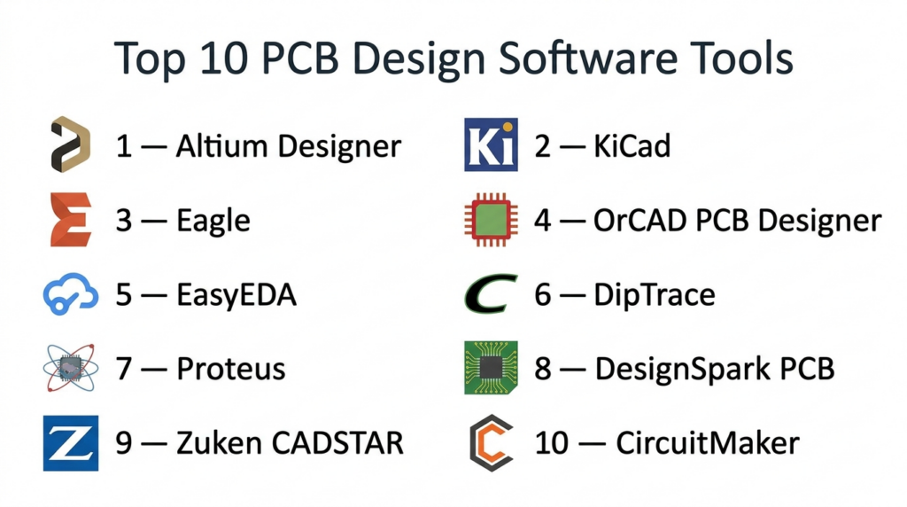
Top 10 PCB Design Software Tools
#1 — Altium Designer
Short description (2–3 lines): A professional PCB design platform known for its powerful layout tools, 3D visualization, and enterprise-grade capabilities.
Key Features
- Advanced PCB layout and routing
- Real-time 3D visualization
- Design rule checking
- Integrated BOM management
- Component libraries
- Collaboration tools
Pros
- Comprehensive feature set
- Strong visualization capabilities
Cons
- Expensive
- High system requirements
Platforms / Deployment
Windows; Self-hosted
Security & Compliance
Not publicly stated
Integrations & Ecosystem
Well-integrated ecosystem for PCB workflows.
- Component libraries
- Manufacturing tools
- APIs
Support & Community
Large user base with extensive documentation and support.
#2 — KiCad
Short description (2–3 lines): A popular open-source PCB design tool offering strong capabilities for both beginners and professionals.
Key Features
- Schematic capture
- PCB layout editor
- 3D viewer
- SPICE simulation
- BOM generation
- Plugin support
Pros
- Free and open-source
- Strong community
Cons
- UI less polished
- Limited enterprise features
Platforms / Deployment
Windows / macOS / Linux; Self-hosted
Security & Compliance
Not publicly stated
Integrations & Ecosystem
Open ecosystem with flexibility.
- Plugins
- Python scripting
- Third-party tools
Support & Community
Active global community with regular updates.
#3 — Eagle
Short description (2–3 lines): A widely used PCB design tool known for simplicity and integration with broader CAD ecosystems.
Key Features
- Schematic capture
- PCB layout
- Autorouting
- Component libraries
- Design rule checks
- Integration with CAD tools
Pros
- Easy to learn
- Good integration ecosystem
Cons
- Limited advanced features
- Subscription model
Platforms / Deployment
Windows / macOS / Linux; Self-hosted
Security & Compliance
Not publicly stated
Integrations & Ecosystem
Part of a broader CAD ecosystem.
- CAD tools
- Libraries
- APIs
Support & Community
Strong community and learning resources.
#4 — OrCAD PCB Designer
Short description (2–3 lines): A reliable PCB design suite offering schematic capture, simulation, and layout tools.
Key Features
- Schematic capture
- PCB layout
- Simulation tools
- Design rule checks
- Component libraries
- Integration with advanced tools
Pros
- Reliable performance
- Good simulation features
Cons
- Windows-only
- Licensing cost
Platforms / Deployment
Windows; Self-hosted
Security & Compliance
Not publicly stated
Integrations & Ecosystem
Part of Cadence ecosystem.
- Simulation tools
- PCB tools
- APIs
Support & Community
Strong documentation and enterprise support.
#5 — EasyEDA
Short description (2–3 lines): A cloud-based PCB design tool designed for simplicity and fast prototyping.
Key Features
- Browser-based design
- Schematic capture
- PCB layout
- SPICE simulation
- Component libraries
- Manufacturing integration
Pros
- Easy to use
- No installation required
Cons
- Limited advanced features
- Internet dependency
Platforms / Deployment
Web; Cloud
Security & Compliance
Not publicly stated
Integrations & Ecosystem
Cloud-native ecosystem.
- Component libraries
- Manufacturing integration
- APIs
Support & Community
Growing user base and documentation.
#6 — DipTrace
Short description (2–3 lines): A user-friendly PCB design tool with strong routing and visualization capabilities.
Key Features
- Schematic capture
- PCB layout
- Autorouting
- 3D preview
- Component editor
- Pattern editor
Pros
- Easy to learn
- Good visualization
Cons
- Limited advanced features
- Smaller ecosystem
Platforms / Deployment
Windows / macOS / Linux; Self-hosted
Security & Compliance
Not publicly stated
Integrations & Ecosystem
Supports design workflows.
- Component libraries
- Export tools
- APIs
Support & Community
Moderate community support.
#7 — Proteus
Short description (2–3 lines): A PCB design and simulation tool widely used for embedded system development and prototyping.
Key Features
- Schematic capture
- PCB layout
- Microcontroller simulation
- Debugging tools
- Component libraries
- Virtual prototyping
Pros
- Strong simulation features
- Good for embedded projects
Cons
- Limited advanced PCB features
- Windows-focused
Platforms / Deployment
Windows; Self-hosted
Security & Compliance
Not publicly stated
Integrations & Ecosystem
Supports embedded workflows.
- Microcontroller libraries
- Simulation tools
- APIs
Support & Community
Good support and documentation.
#8 — DesignSpark PCB
Short description (2–3 lines): A free PCB design tool aimed at hobbyists and engineers for quick design and prototyping.
Key Features
- Schematic capture
- PCB layout
- Component libraries
- Design rule checks
- BOM tools
- Export features
Pros
- Free to use
- Easy for beginners
Cons
- Limited advanced capabilities
- Smaller ecosystem
Platforms / Deployment
Windows; Self-hosted
Security & Compliance
Not publicly stated
Integrations & Ecosystem
Basic ecosystem support.
- Libraries
- Export tools
- Extensions
Support & Community
Moderate support and resources.
#9 — Zuken CADSTAR
Short description (2–3 lines): A professional PCB design tool focused on complex designs and signal integrity.
Key Features
- Schematic design
- PCB layout
- Signal integrity analysis
- Autorouting
- Design rule checks
- Manufacturing outputs
Pros
- Strong for complex boards
- Reliable performance
Cons
- Older interface
- Limited ecosystem
Platforms / Deployment
Windows; Self-hosted
Security & Compliance
Not publicly stated
Integrations & Ecosystem
Part of Zuken ecosystem.
- CAD tools
- APIs
- Manufacturing tools
Support & Community
Professional support available.
#10 — CircuitMaker
Short description (2–3 lines): A free PCB design tool focused on community-driven development and collaboration.
Key Features
- Schematic capture
- PCB layout
- Community component libraries
- Design sharing
- Basic simulation
- Collaboration tools
Pros
- Free to use
- Strong community
Cons
- Limited advanced features
- Cloud dependency
Platforms / Deployment
Windows; Cloud
Security & Compliance
Not publicly stated
Integrations & Ecosystem
Community-driven ecosystem.
- Shared libraries
- Design sharing
- APIs
Support & Community
Active community support.
Comparison Table (Top 10)
| Tool Name | Best For | Platform(s) Supported | Deployment | Standout Feature | Public Rating |
|---|---|---|---|---|---|
| Altium Designer | Professional PCB design | Windows | Self-hosted | 3D visualization | N/A |
| KiCad | Open-source users | Win/macOS/Linux | Self-hosted | Free platform | N/A |
| Eagle | Beginners & SMB | Win/macOS/Linux | Self-hosted | Ease of use | N/A |
| OrCAD PCB Designer | Mid-market PCB | Windows | Self-hosted | Simulation tools | N/A |
| EasyEDA | Cloud design | Web | Cloud | Browser-based | N/A |
| DipTrace | SMB users | Win/macOS/Linux | Self-hosted | 3D preview | N/A |
| Proteus | Embedded design | Windows | Self-hosted | Microcontroller simulation | N/A |
| DesignSpark PCB | Hobbyists | Windows | Self-hosted | Free tool | N/A |
| CADSTAR | Complex boards | Windows | Self-hosted | Signal integrity | N/A |
| CircuitMaker | Community users | Windows | Cloud | Design sharing | N/A |
Evaluation & Scoring of PCB Design Software
| Tool Name | Core (25%) | Ease (15%) | Integrations (15%) | Security (10%) | Performance (10%) | Support (10%) | Value (15%) | Weighted Total |
|---|---|---|---|---|---|---|---|---|
| Altium Designer | 9 | 8 | 9 | 6 | 9 | 9 | 6 | 8.2 |
| KiCad | 7 | 7 | 7 | 5 | 7 | 8 | 10 | 7.6 |
| Eagle | 7 | 8 | 7 | 5 | 7 | 7 | 7 | 7.1 |
| OrCAD | 8 | 7 | 8 | 6 | 8 | 8 | 7 | 7.7 |
| EasyEDA | 7 | 9 | 7 | 5 | 7 | 7 | 9 | 7.8 |
| DipTrace | 7 | 8 | 7 | 5 | 7 | 7 | 8 | 7.4 |
| Proteus | 8 | 7 | 7 | 5 | 8 | 7 | 7 | 7.3 |
| DesignSpark PCB | 6 | 8 | 6 | 5 | 6 | 6 | 9 | 6.9 |
| CADSTAR | 8 | 6 | 7 | 6 | 8 | 7 | 6 | 7.2 |
| CircuitMaker | 6 | 8 | 6 | 5 | 6 | 7 | 9 | 6.9 |
How to interpret scores:
- Scores reflect relative strengths across criteria
- Higher scores indicate balanced capabilities
- Enterprise tools excel in performance and features
- Open-source tools offer better value
- Use this as a shortlisting guide, not a final decision
Which PCB Design Software Tool Is Right for You?
Solo / Freelancer
- Best: KiCad, EasyEDA
- Low cost and easy to start
SMB
- Best: DipTrace, Eagle
- Balanced features and usability
Mid-Market
- Best: OrCAD, Proteus
- Good simulation and performance
Enterprise
- Best: Altium Designer, CADSTAR
- Advanced features and scalability
Budget vs Premium
- Budget: KiCad, DesignSpark
- Premium: Altium
Feature Depth vs Ease of Use
- Deep: Altium, CADSTAR
- Easy: EasyEDA, DipTrace
Integrations & Scalability
- Strong: Altium, OrCAD
- Flexible: KiCad
Security & Compliance Needs
- Enterprise: Altium
- Basic: Open-source tools
Frequently Asked Questions (FAQs)
What is PCB design software?
It is used to design and prepare printed circuit boards for manufacturing.
Is PCB software free?
Some tools are free, while others require paid licenses.
Can beginners use PCB tools?
Yes, beginner-friendly tools are available.
What files are used in PCB design?
Common formats include Gerber and BOM files.
Do PCB tools support simulation?
Yes, many tools include simulation features.
Is cloud PCB design safe?
Security varies by tool; check features before use.
Can PCB tools integrate with CAD?
Yes, many tools support MCAD integration.
How long does it take to learn?
Depends on tool complexity and user experience.
What industries use PCB design?
Electronics, automotive, telecom, and aerospace.
Can I switch PCB tools?
Yes, but it may require adapting workflows.
Conclusion
PCB design software is essential for modern electronics development, enabling engineers to create reliable, high-performance circuit boards efficiently. With a wide range of tools available—from open-source platforms to enterprise-grade solutions—there is an option for every type of user.