Find the Best Cosmetic Hospitals — Choose with Confidence
Discover top cosmetic hospitals in one place and take the next step toward the look you’ve been dreaming of.
“Your confidence is your power — invest in yourself, and let your best self shine.”
Compare • Shortlist • Decide smarter — works great on mobile too.
Introduction
Electronic Design Automation (EDA) software refers to a category of tools used to design, simulate, verify, and manufacture electronic systems such as printed circuit boards (PCBs) and integrated circuits (ICs). These tools form a complete workflow that allows engineers to move from concept to production-ready hardware efficiently.
EDA software is essential in modern electronics development because today’s chips and systems are extremely complex, often containing billions of components. These tools help reduce errors, improve performance, and accelerate time-to-market while ensuring reliability.
Common use cases include:
- PCB design and layout for electronics manufacturing
- IC and semiconductor chip design (VLSI, SoC)
- Circuit simulation and verification
- FPGA development and prototyping
- Signal integrity and power analysis
What buyers should evaluate:
- Schematic capture and layout capabilities
- Simulation and verification tools
- Ease of use and learning curve
- Scalability for complex designs
- Integration with manufacturing workflows
- Support for HDL (Verilog, VHDL)
- Cloud vs desktop deployment
- Component libraries and ecosystem
- Automation and scripting features
- Security and collaboration features
Best for: Electronics engineers, hardware designers, semiconductor companies, embedded system developers, and research institutions.
Not ideal for: Non-technical users or teams only needing basic diagramming or electrical visualization tools.
Key Trends in Electronic Design Automation (EDA) Software
- AI-driven chip design and verification workflows improving efficiency
- Cloud-based EDA platforms enabling distributed engineering teams
- Integration of multiphysics simulation (thermal, electrical, mechanical)
- Automation of design verification and testing
- Open-source EDA adoption increasing among startups and academia
- FPGA-first prototyping workflows accelerating hardware validation
- Tighter integration with manufacturing pipelines (DFM, fabrication)
- Support for heterogeneous chip architectures (chiplets, SoCs)
- Subscription-based licensing models replacing traditional licenses
- Security-focused collaboration environments
How We Selected These Tools (Methodology)
- Evaluated industry adoption and market leadership
- Assessed end-to-end design workflow capabilities
- Considered performance and scalability for complex designs
- Reviewed integration with simulation, verification, and manufacturing tools
- Analyzed security posture and enterprise readiness signals
- Included a mix of enterprise, mid-market, and open-source tools
- Evaluated documentation and onboarding experience
- Considered deployment flexibility (cloud and self-hosted)
- Prioritized tools with strong ecosystems and active development
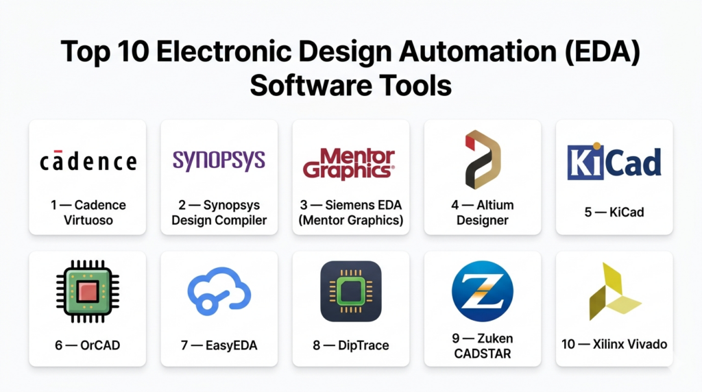
Top 10 Electronic Design Automation (EDA) Software Tools
#1 — Cadence Virtuoso
Short description (2–3 lines): A leading platform for analog and mixed-signal IC design, widely used in semiconductor industries.
Key Features
- Advanced schematic capture and layout
- Analog and RF simulation
- Parasitic extraction
- Constraint-driven design
- Integrated verification tools
- High scalability
Pros
- Industry-standard for IC design
- Strong simulation accuracy
Cons
- Expensive
- Steep learning curve
Platforms / Deployment
Linux; Self-hosted
Security & Compliance
Not publicly stated
Integrations & Ecosystem
Part of a large semiconductor ecosystem.
- Cadence tools
- APIs
- Verification frameworks
Support & Community
Enterprise-grade support and strong professional ecosystem.
#2 — Synopsys Design Compiler
Short description (2–3 lines): A widely used synthesis tool for digital IC design and optimization.
Key Features
- RTL synthesis
- Timing optimization
- Power optimization
- Scalability for large designs
- Integration with verification tools
- HDL support
Pros
- Industry-leading synthesis capabilities
- High performance
Cons
- Complex setup
- High cost
Platforms / Deployment
Linux; Self-hosted
Security & Compliance
Not publicly stated
Integrations & Ecosystem
Part of Synopsys suite.
- Verification tools
- Simulation tools
- APIs
Support & Community
Strong enterprise support.
#3 — Siemens EDA (Mentor Graphics)
Short description (2–3 lines): A comprehensive EDA suite covering PCB design, IC design, and verification.
Key Features
- PCB design tools
- IC verification
- Simulation tools
- Signal integrity analysis
- Design automation
- Multidomain support
Pros
- Broad tool coverage
- Strong enterprise capabilities
Cons
- Expensive
- Complex workflows
Platforms / Deployment
Windows / Linux; Self-hosted
Security & Compliance
Not publicly stated
Integrations & Ecosystem
Part of Siemens ecosystem.
- PLM tools
- Simulation tools
- APIs
Support & Community
Enterprise-level support and documentation.
#4 — Altium Designer
Short description (2–3 lines): A leading PCB design platform known for ease of use and strong visualization tools.
Key Features
- PCB layout and routing
- Schematic capture
- 3D visualization
- Component libraries
- Design rule checks
- Collaboration tools
Pros
- User-friendly interface
- Strong PCB capabilities
Cons
- Expensive
- Resource-intensive
Platforms / Deployment
Windows; Self-hosted
Security & Compliance
Not publicly stated
Integrations & Ecosystem
Strong PCB ecosystem.
- Component libraries
- Manufacturing tools
- APIs
Support & Community
Large community and strong documentation.
#5 — KiCad
Short description (2–3 lines): A free and open-source EDA suite for PCB design and simulation.
Key Features
- Schematic capture
- PCB layout
- SPICE simulation
- 3D visualization
- BOM generation
- Open-source extensibility
Pros
- Free and accessible
- Strong community
Cons
- Less polished UI
- Limited enterprise features
Platforms / Deployment
Windows / macOS / Linux; Self-hosted
Security & Compliance
Not publicly stated
Integrations & Ecosystem
Open ecosystem.
- Plugins
- Python scripting
- Third-party tools
Support & Community
Large global community and active development.
#6 — OrCAD
Short description (2–3 lines): A PCB design tool suite focused on schematic capture and simulation.
Key Features
- Schematic capture
- PCB layout
- Simulation tools
- Component libraries
- Design rule checks
- Integration with Cadence tools
Pros
- Reliable and widely used
- Good simulation capabilities
Cons
- Windows-only
- Licensing cost
Platforms / Deployment
Windows; Self-hosted
Security & Compliance
Not publicly stated
Integrations & Ecosystem
Part of Cadence ecosystem.
- Simulation tools
- PCB tools
- APIs
Support & Community
Strong documentation and support.
#7 — EasyEDA
Short description (2–3 lines): A web-based EDA platform for schematic capture, simulation, and PCB design.
Key Features
- Browser-based design
- SPICE simulation
- PCB layout tools
- Component libraries
- Collaboration features
- Manufacturing integration
Pros
- No installation required
- Easy to use
Cons
- Limited advanced features
- Internet dependency
Platforms / Deployment
Web; Cloud
Security & Compliance
Not publicly stated
Integrations & Ecosystem
Cloud-based ecosystem.
- Component libraries
- Manufacturing services
- APIs
Support & Community
Growing community and documentation.
#8 — DipTrace
Short description (2–3 lines): A user-friendly PCB design tool with strong visualization and routing features.
Key Features
- Schematic capture
- PCB layout
- 3D preview
- Autorouting
- Component editor
- Pattern editor
Pros
- Easy to learn
- Good visualization tools
Cons
- Limited advanced features
- Smaller ecosystem
Platforms / Deployment
Windows / macOS / Linux; Self-hosted
Security & Compliance
Not publicly stated
Integrations & Ecosystem
Supports design workflows.
- Component libraries
- Export tools
- APIs
Support & Community
Moderate community support.
#9 — Zuken CADSTAR
Short description (2–3 lines): A PCB design tool for complex multilayer boards and signal integrity analysis.
Key Features
- Schematic design
- PCB layout
- Signal integrity analysis
- Design rule checks
- Autorouting
- Manufacturing outputs
Pros
- Strong PCB capabilities
- Suitable for complex designs
Cons
- Older interface
- Limited ecosystem
Platforms / Deployment
Windows; Self-hosted
Security & Compliance
Not publicly stated
Integrations & Ecosystem
Part of Zuken ecosystem.
- CAD tools
- APIs
- Manufacturing tools
Support & Community
Professional support available.
#10 — Xilinx Vivado
Short description (2–3 lines): A leading FPGA design suite used for synthesis, simulation, and hardware debugging.
Key Features
- FPGA synthesis and implementation
- Timing analysis
- Hardware debugging
- Simulation tools
- IP core integration
- Design automation
Pros
- Strong FPGA support
- Integrated workflow
Cons
- Vendor-specific
- Resource-intensive
Platforms / Deployment
Windows / Linux; Self-hosted
Security & Compliance
Not publicly stated
Integrations & Ecosystem
Part of FPGA ecosystem.
- IP cores
- Development tools
- APIs
Support & Community
Strong documentation and developer community.
Comparison Table (Top 10)
| Tool Name | Best For | Platform(s) Supported | Deployment | Standout Feature | Public Rating |
|---|---|---|---|---|---|
| Cadence Virtuoso | IC design | Linux | Self-hosted | Analog/RF design | N/A |
| Synopsys Design Compiler | Digital IC | Linux | Self-hosted | RTL synthesis | N/A |
| Siemens EDA | Enterprise workflows | Win/Linux | Self-hosted | Full EDA suite | N/A |
| Altium Designer | PCB design | Windows | Self-hosted | 3D PCB design | N/A |
| KiCad | Open-source PCB | Win/macOS/Linux | Self-hosted | Free platform | N/A |
| OrCAD | PCB design | Windows | Self-hosted | Simulation tools | N/A |
| EasyEDA | Cloud PCB | Web | Cloud | Browser-based | N/A |
| DipTrace | SMB PCB | Win/macOS/Linux | Self-hosted | 3D preview | N/A |
| CADSTAR | Complex PCB | Windows | Self-hosted | Signal integrity | N/A |
| Vivado | FPGA design | Win/Linux | Self-hosted | FPGA workflow | N/A |
Evaluation & Scoring of Electronic Design Automation (EDA) Software
| Tool Name | Core (25%) | Ease (15%) | Integrations (15%) | Security (10%) | Performance (10%) | Support (10%) | Value (15%) | Weighted Total |
|---|---|---|---|---|---|---|---|---|
| Cadence Virtuoso | 10 | 5 | 9 | 7 | 10 | 9 | 5 | 8.1 |
| Synopsys Design Compiler | 10 | 5 | 9 | 7 | 10 | 9 | 5 | 8.1 |
| Siemens EDA | 9 | 6 | 9 | 7 | 9 | 9 | 6 | 8.2 |
| Altium Designer | 8 | 8 | 8 | 6 | 8 | 8 | 7 | 7.9 |
| KiCad | 7 | 7 | 7 | 5 | 7 | 7 | 10 | 7.5 |
| OrCAD | 8 | 7 | 8 | 6 | 8 | 8 | 7 | 7.8 |
| EasyEDA | 7 | 9 | 7 | 5 | 7 | 7 | 9 | 7.8 |
| DipTrace | 7 | 8 | 7 | 5 | 7 | 7 | 8 | 7.4 |
| CADSTAR | 8 | 6 | 7 | 6 | 8 | 7 | 6 | 7.2 |
| Vivado | 9 | 6 | 8 | 6 | 9 | 8 | 6 | 7.9 |
How to interpret scores:
- Scores are comparative and reflect overall balance across tools
- Higher scores indicate stronger performance across multiple criteria
- Enterprise tools tend to excel in performance but may lag in ease of use and value
- Open-source tools score higher in value but may require more expertise
- Use this scoring model to shortlist tools based on your priorities
Which Electronic Design Automation (EDA) Software Tool Is Right for You?
Solo / Freelancer
- Best: KiCad, EasyEDA
- These tools are cost-effective, easy to start with, and flexible for small projects
SMB
- Best: DipTrace, Altium Designer
- Provide a balance of usability, features, and scalability for growing teams
Mid-Market
- Best: OrCAD, CADSTAR
- Offer strong PCB design and simulation capabilities with moderate complexity
Enterprise
- Best: Cadence Virtuoso, Synopsys Design Compiler, Siemens EDA
- Designed for large-scale IC design, verification, and manufacturing workflows
Budget vs Premium
- Budget: KiCad, EasyEDA
- Premium: Cadence, Synopsys
Feature Depth vs Ease of Use
- Deep features: Cadence, Synopsys
- Ease of use: EasyEDA, DipTrace
Integrations & Scalability
- Strong ecosystems: Synopsys, Siemens
- Flexible options: Open-source tools like KiCad
Security & Compliance Needs
- Enterprise-level: Cadence, Siemens
- Basic needs: Open-source and smaller tools
Frequently Asked Questions (FAQs)
What is EDA software used for?
EDA software is used to design, simulate, and verify electronic systems such as PCBs and integrated circuits.
Is EDA software expensive?
Enterprise tools can be expensive, while open-source tools are available at no cost.
Can beginners use EDA tools?
Yes, beginner-friendly tools exist, but advanced tools require training and experience.
What industries use EDA?
Industries include semiconductor, electronics, automotive, aerospace, and telecommunications.
Does EDA software support simulation?
Yes, simulation and verification are core features in most EDA tools.
Can EDA tools run on the cloud?
Yes, some modern tools offer cloud-based deployment and collaboration.
What languages are used in EDA?
Common languages include Verilog and VHDL for hardware description.
Is open-source EDA reliable?
Yes, open-source tools are reliable for many use cases, especially learning and small projects.
How long does it take to learn EDA?
Learning time varies depending on tool complexity and user experience.
Can I switch EDA tools easily?
Switching is possible but may require retraining and adapting workflows.
Conclusion
Electronic Design Automation (EDA) software is a critical component of modern electronics and semiconductor development. These tools enable engineers to handle complex designs, improve accuracy, and accelerate development cycles across a wide range of applications.
From enterprise-grade platforms to accessible open-source solutions, each tool offers unique strengths depending on your needs. The right choice depends on your project complexity, budget, and workflow requirements.